Teledyne DALSA offers industry-leading manufacturing capability for high-performance CCD fabrication process with a long history of excellence.
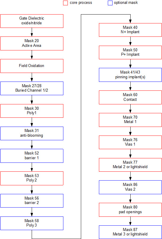
Teledyne DALSA Semiconductor’s 150mm CCD process offers surface or buried channel operation at up to 15V with two or three layers of polysilicon and one, two or three layers of metal. A modular processing approach allows our foundry customers to adjust process parameters to meet the most demanding requirements for CTE (>99.999%), charge storage capacity, and dark current (<1nA/cm2). The base process uses 1X projection lithography with 2.5µm design rules, allowing die sizes of up to 100mm X 100mm. Where required, tighter alignment tolerances and smaller feature sizes can be obtained by using 5X lithography, using a mix and match or all-stepper approach. The maximum die size attainable with the stepper is 22mm X 22mm, but larger sensors can be fabricated using stitching.
Our CCD technology can be extensively tuned; p or n-type, bulk or epi starting material can be specified over a wide range of resistivity, including float zone silicon up to 10kΩ-cm. Customers specify the buried channel and barrier implants which suit their application; channel stops, anti-blooming implants or other special features can be added. Successful projects have included rad-hard PMOS CCDs, and the world’s highest resolution monolithic device at over 250MP.
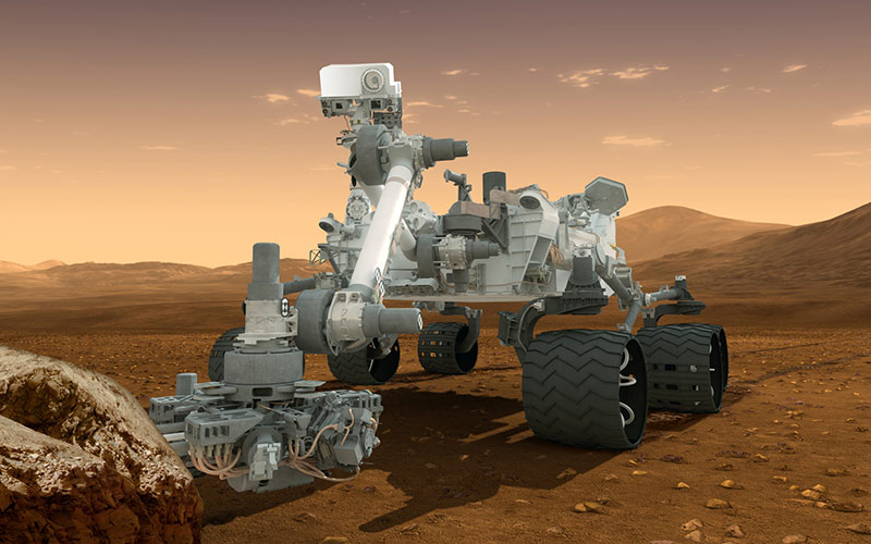
Typical applications are industrial and scientific, including aerial and satellite imaging. Custom variants of this process supply many of the image sensors used in the industry-leading digital cameras of Teledyne DALSA's Machine Vision division. NASA's JPL chose Teledyne DALSA to fabricate several of the image sensors on the Curiosity Mars Rover, just as it did for the earlier Spirit and Opportunity Rovers.
To support all our customers' custom CCD processes, we offer a wide range of services from mask manufacturing to complete device characterization.
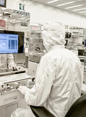
Teledyne DALSA Semiconductor operates its CCD Wafer Foundry Service as a separate arm from any of the other Teledyne DALSA group of Business Units. Customer information and data confidentiality is assured.
| Scanner Version | Stepper Version | ||
|---|---|---|---|
|
Poly 1/2/3
|
width |
2.5µm |
2.5µm |
| spacing |
2.5µm |
2.5µm |
|
|
Overlap Poly2/1 or Poly 3/2 |
0.5µm |
0.3µm |
|
|
Contact size |
2.5µm X 2.5µm 2.5µm |
1.0µm X 1.0µm |
|
|
Via size |
3.0µm X 3.0µm |
1.0µm X 1.0µm |
|
|
Metal 1
|
width |
3.0µm |
1.1µm |
| spacing |
3.0µm |
1.0µm |
|
|
Metal 2
|
width (dry/wet etch) |
3.0µm / 4.0µm* |
1.2µm |
| spacing (dry/wet etch) |
4.0µm / 5.0µm* |
1.1µm |
|
|
Metal 3
|
width |
5µm |
2.0µm |
| spacing |
5µm |
1.8µm |
|
|
Gate dielectric thickness |
500Å |
500Å |
|
|
Interpoly dielectric thickness |
3000Å |
3000Å |
|
|
N+ junction depth |
0.5µm |
0.5µm |
*Wet metal etch option.
Contact Teledyne DALSA Semiconductor to receive our most recent detailed design rules document.
Questions? Need more info? Contact our sales team about our foundry products and services today.
Contact us