TSVs are high performance interconnect techniques that are key enabling technologies for 3D integration of MEMS. Compared to 3D techniques such as flip chips, wire bonds, or package-on-package, the density of through-silicon vias is substantially higher, and the length of the connections is shorter. Teledyne DALSA is pleased to offer both silicon and copper TSVs. Each has its particular strength. Teledyne DALSA is pleased to offer both silicon and copper TSVs; our sister foundry Teledyne Micralyne offers polysilicon and metal TSVs. Each TSV type has its particular strength.
TSVs are usually categorized as ‘Via-First’ or ‘Via-Last’, the main differentiator being that via-first take place before wafer bonding and are able to withstand temperatures of several hundred degrees. Via-last are post bonding, and typically the temperatures involved need to be low enough to prevent damage to back-end CMOS layers.
 Copper filled 5µm wide trench before planarization
Teledyne-DALSA Via–First TSVs can use the trench fill (in-situ doped poly) as the conductor, or if larger vias are required, the conductive region can be the MEMs wafer itself, in which case the trenches are used only to provide isolation. This technology is available for both 150mm and 200mm wafers.

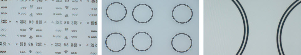
Teledyne DALSA’s Via-Last technology utilizes copper vias, filled using the aveni low temperature electrochemical process. This technology produces perfect filling of 100 µm deep vias only 5µm diameter, which connect to the outside world through a copper redistribution layer and Ni/Au UBM.
Surface mountable 3D ICs use wafer level packaging for dramatic size and form factor reduction with corresponding cost reductions, making them ideal for mobile applications. Teledyne DALSA offers advanced I/O options including µBGA, solderable pads, or standard pads for stacked die and co-package designs, with hermetic seals for oscillators, pressure and image sensors, and non hermetic for RF filters, microfluidics and Si microphones.
